Driving Excellence Through Innovation
Advanced Material Solutions for Next-Gen Technologies
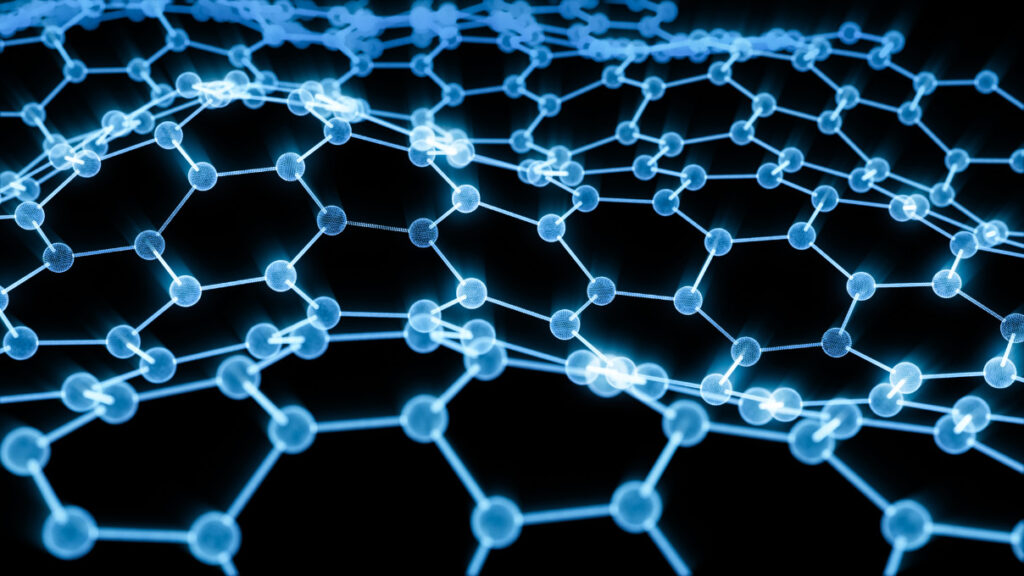
Sics Direct Co., Ltd. is a leading innovator in advanced material science, specializing in multi-dimension materials, CS graphene devices, CS single crystal growth, thermal field design, and high-precision inspection tools. Our cutting-edge technologies enable seamless integration into semiconductor, optoelectronics, and next-generation electronic applications.
01
Multi-dimension material
02
CS Graphene device
Industry Solutions
05
Thermal field design
04
CS Single crystal growth
06
Inspection tools
Product Feature
Driving Future Innovation
Advanced Material Engineering
Tailored solutions for high-performance applications in semiconductors and electronics.
Enhanced Structural Integrity
Superior durability and precision for next-generation devices.
Scalability & Customization
Designed to meet specific industry needs with flexible manufacturing capabilities.
Sustainable & High-Purity Solutions
Developed with eco-friendly production methods for long-term reliability.
High Conductivity & Strength
Delivers superior electrical and mechanical performance.
Ultra-Thin & Lightweight Design
Enables flexible and compact device integration.
Advanced Manufacturing Techniques
Ensures high-purity, defect-free graphene production.
Scalable & Cost-Effective Solutions
Supports mass production for commercial and industrial use.
High-Purity Crystals for Semiconductors
Essential for power electronics and optoelectronic applications.
Low Defect Density
Ensures high-performance and reliable device operation.
Precision-Controlled Growth Techniques
Supports the development of SiC, GaN, and other advanced semiconductors.
Enhanced Efficiency & Yield
Reduces material waste and improves cost-effectiveness.
Optimized Heat Management
Improves thermal stability for high-performance devices.
Innovative Simulation & Modeling
Ensures precision in temperature distribution.
Enhanced Energy Efficiency
Reduces power consumption while maintaining peak performance.
Scalable for Industrial Use
Suitable for both research and large-scale manufacturing environments.
Nanometer-Level Accuracy
Ensures precise measurement for semiconductor and advanced material applications.
Automated Defect Detection
Enhances quality control and reduces production errors. Improves efficiency in manufacturing processes.
Multi-Functional Inspection Capabilities
Supports diverse applications including crystal growth, graphene production, and thermal field assessment.
Reliable & Scalable Technology
Adaptable for both R&D and high-volume production lines.
JOIN US
Explore the Future Growth
empower the innovations
Our Happy Partners